
Rigid-Flex PCB Design Guidelines for High-Density and High-Speed Applications
Rigid-Flex PCB design has revolutionized the electronic industry, particularly for high-density and high-speed applications.
This innovative approach combines the advantageous characteristics of rigid and flexible printed circuit boards (PCBs), enabling designers to create compact, lightweight, and efficient electronic solutions.
Whether it’s for aerospace, medical devices, or telecommunications, understanding the guidelines for crafting effective rigid-flex PCB layouts is critical for engineers and designers striving for optimal performance.
Understanding Rigid-Flex PCBs
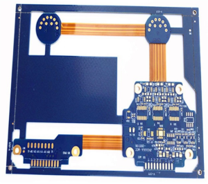
Rigid-flex PCBs merge rigid and flexible substrates into a single package, allowing for complex designs and enhanced functionality.
Unlike traditional rigid or flexible boards, the integration of these two elements leads to reduced assembly costs, improved signal integrity, and increased reliability.
Application Areas:
- Medical Devices: Devices such as pacemakers and imaging systems benefit from the compactness and flexibility of rigid-flex designs.
- Consumer Electronics: Smartphones and tablets utilize rigid-flex PCBs for multi-layered designs without compromising aesthetics and performance.
- Aerospace and Defense: Rigid-flex technology withstands the extreme conditions of aerospace applications while providing necessary functionality.
Key Design Guidelines for High-Density Applications
When tackling high-density designs, effective layout planning is paramount. Here are essential guidelines to keep in mind:
Layer Stack-Up
The layer stack-up is crucial in a rigid-flex design. Utilizing a defined stack—typically alternating between layer types—will allow for the optimized routing of high-frequency signals.
The common configurations often include buried and blind vias, and it’s important to strategize where these vias will be placed to maintain signal integrity.
Routing Techniques
Rigid-flex PCBs often require complex routing strategies owing to the high-density nature of the applications.
Employ differential pair routing for signals that need to maintain integrity over distance. Keeping the space between the pairs uniform will minimize electromagnetic interference.
Additionally, using controlled impedance traces can help ensure that signals maintain their original characteristics throughout their travel.
High-Speed Design Considerations
As applications demand faster data rates, attention to high-speed design guidelines becomes critical. Here are fundamental aspects that shouldn’t be overlooked:
Signal Integrity
In high-speed applications, signal integrity is of utmost concern.
Designers should use shorter trace lengths wherever possible, avoiding sharp corners that could lead to reflections.
Incorporating ground planes and return paths alongside critical signal lines can help minimize unwanted coupling and noise.
Controlled Impedance
Maintaining controlled impedance is vital in high-speed rigid-flex designs.
Careful attention should be paid to trace width and spacing, depending on the materials chosen for the substrate.
Utilizing advanced simulation tools can provide valuable insights into the impedance characteristics, allowing designers to adjust their designs accordingly.
Material Selection
Selecting the right materials is essential when designing for high-density and high-speed applications.
The following materials are often favored:
Dielectric Materials
Low-loss dielectric materials, such as PTFE or FR-4 with a low dielectric constant, are preferred due to their improved electrical performance at high frequencies.
This contributes to better signal integrity and efficiency.
Copper Thickness
Using thinner copper layers can help reduce capacitance and improve high-frequency performance.
Designers often opt for copper thickness ranging from 1 to 2 oz. per square foot to achieve the desired balance between rigidity and flexibility.
Testing and Validation
After the design and manufacturing phases, testing and validation become crucial steps.
Employing high-frequency simulation tools can offer insights into how the PCB will behave in real-world conditions.
Power Integrity Testing
Power integrity tests ensure that power delivery networks (PDN) work optimally, providing a stable voltage to components under various conditions.
Monitoring voltage drop and ripple during operation can help identify potential issues before the product reaches the market.
Signal Integrity Analysis
Conducting thorough signal integrity tests will ascertain the effectiveness of the design.
This analysis often includes eye diagram measurements and time delay assessments, which can help highlight any problems in the transmission paths.
Conclusion
Designing rigid-flex PCBs for high-density and high-speed applications is a complex yet rewarding endeavor.
By following these guidelines on layer stack-up, routing techniques, material selection, and thorough testing, designers can enhance their products’ performance and reliability.
The evolution of rigid-flex technology will continue to push the boundaries of electronic capabilities, allowing for even more compact and sophisticated devices in the future.
Embracing these guidelines is key to driving innovation and achieving excellence in the competitive landscape of modern electronics.