
Rigid-Flex PCB Design Guidelines for High-Density and High-Speed Applications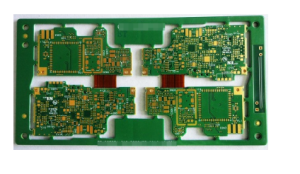
Rigid-flex PCB design is essential for modern electronics, especially in applications demanding both high density and high-speed performance.
These innovative printed circuit boards combine the advantages of rigid and flexible circuits, enabling manufacturers to achieve intricate designs, save space, and enhance the reliability of their products.
As industries shift toward miniaturization and complex functionality, understanding the guidelines for designing rigid-flex PCBs becomes pivotal.
Understanding Rigid-Flex Technology
At its core, rigid-flex technology integrates rigid boards and flexible circuits into a single assembly.
This combination offers unparalleled versatility, making it ideal for compact electronic devices such as smartphones, medical equipment, and aerospace applications.
The ability to configure components in a 3D space allows designers to maximize available real estate while maintaining functionality.
Key Considerations in Rigid-Flex PCB Design
When embarking on a rigid-flex PCB design, several critical factors must be considered to ensure optimal performance:
1. Material Selection
Choosing the appropriate materials is paramount in achieving both high-speed and high-density goals. Typical materials include:
- Dielectric Materials: Ensure low dielectric constant and loss to maintain signal integrity.
- Flex Materials: Select materials that can withstand bending and twisting without compromising performance.
Polyimide is a popular choice due to its excellent thermal stability and chemical resistance. - Surface Finish: The appropriate surface finish will enhance solderability and protect against oxidation.
Consider finishes like ENIG (Electroless Nickel Immersion Gold) for durability and reliability.
2. Layer Stack-Up Design
Layer stack-up plays a critical role in managing electromagnetic interference (EMI) and controlling impedance.
In high-speed applications, maintaining a consistent dielectric thickness is essential.
Opt for a design that allows for adequate ground planes, power distribution, and signal routing.
An effective stack-up could include alternating layers of rigid and flexible sections, optimizing both electrical and mechanical performance.
3. Impedance Control
Impedance control is crucial for high-speed signals as it affects signal integrity. Designing transmission lines with controlled impedance requires careful attention to trace width, spacing, and dielectric constant.
Utilize simulation tools to model impedance profiles and make necessary adjustments to minimize reflections and ensure reliable communication between components.
Design Guidelines for High-Density Applications
High-density applications push the limits of what rigid-flex PCBs can achieve.
Several guidelines help maximize space utilization while ensuring functionality:
1. Trace Width and Spacing
Utilize thinner traces and smaller pad sizes to pack more components into a compact area.
However, it’s vital to adhere to industry standards regarding minimum trace width and spacing, especially when dealing with high-frequency signals.
2. Via Design
Using microvias can significantly enhance space efficiency. Microvias allow for smaller connection points between layers.
Employ staggered microvias for optimal routing and minimize signal loss. Ensure that your design maintains via aspect ratios that comply with manufacturer capabilities.
3. Component Placement
Strategically place components to optimize thermal management and minimize cross-talk.
Prioritize the placement of high-speed components near the signal source and ensure power and ground connections are robust.
Testing and Validation
Once your rigid-flex PCB is designed, thorough testing is essential. Employ techniques like:
- DC and AC Testing: Evaluate performance under various frequencies.
- Thermal Cycling: Assess the ability to withstand temperature fluctuations common in high-speed applications.
- Mechanical Flexibility Tests: Ensure the board can endure bending and twisting without failure.
Proper validation helps identify potential issues early in the production process, minimizing costly redesigns.
Conclusion
Rigid-flex PCB design is a complex and rewarding endeavor, especially within high-density and high-speed applications.
By adhering to these guidelines on material selection, layer stack-up, impedance control, and testing methodologies, designers can create robust and reliable circuits that meet the demands of modern technology.
As the push for miniaturization continues, mastering rigid-flex PCB design will be instrumental in pushing the boundaries of what’s possible in electronics.