
Benefits of Using Laser Direct Imaging for Rigid Flex PCB Assembly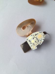
In the rapidly evolving world of Internet of Things (IoT) devices, the demand for smaller, more efficient, and more reliable electronics is constantly increasing.
Rigid flex PCBs have emerged as a popular choice for manufacturers looking to meet these demands, as they offer a combination of flexibility and durability that traditional rigid PCBs cannot match.
However, assembling rigid flex PCBs can be a complex and challenging process, requiring innovative techniques to ensure high-quality results.
One of the key steps in the assembly of rigid flex PCBs is the imaging of the circuit patterns onto the board.
Traditionally, this process has been done using photolithography, which involves exposing a photosensitive material to UV light through a mask to create the circuit patterns.
While this method has been effective for many years, it has its limitations, particularly when it comes to the precision and accuracy required for modern IoT devices.
This is where laser direct imaging (LDI) comes in.
LDI is a cutting-edge technology that uses a laser to directly expose the circuit patterns onto the PCB, eliminating the need for masks and significantly improving the accuracy and resolution of the imaging process.
By using LDI for rigid flex PCB assembly, manufacturers can achieve tighter tolerances, finer features, and higher yields, leading to a more reliable and cost-effective end product.
One of the key benefits of using LDI for rigid flex PCB assembly is its ability to handle complex designs with ease.
With traditional photolithography, intricate patterns and fine features can be difficult to achieve, leading to potential defects and reliability issues in the final product.
LDI, on the other hand, excels at producing high-resolution images with exceptional precision, allowing manufacturers to create even the most intricate designs with confidence.
Another advantage of LDI is its speed and efficiency.
Traditional photolithography can be a time-consuming process, requiring multiple steps and careful alignment of masks. In contrast,
LDI is a one-step process that can be completed in a fraction of the time, reducing production lead times and increasing overall throughput.
This not only saves time and money for manufacturers but also allows them to respond more quickly to changing market demands.
In addition to its precision and efficiency, LDI also offers improved consistency and repeatability in the imaging process.
With traditional photolithography, variations in exposure times, mask alignment, and other factors can lead to inconsistencies in the final product.
LDI eliminates these variables, ensuring that each PCB is produced to the same high standard every time.
This level of consistency is essential for meeting the strict quality requirements of IoT devices and other high-tech applications.
Overall, the benefits of using LDI for rigid flex PCB assembly are clear.
From its ability to handle complex designs with precision to its speed, efficiency, and consistency, LDI offers a superior imaging solution for manufacturers looking to produce high-quality IoT devices.
By embracing this innovative technology, manufacturers can stay ahead of the competition and deliver reliable, cost-effective products that meet the demands of today’s fast-paced electronics market.