
Essential Rigid-Flex PCB Design Guidelines for Optimal Performance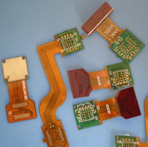
Essential rigid-flex PCB design guidelines are crucial for ensuring that your printed circuit boards function effectively and efficiently.
Rigid-flex PCBs combine the best of both rigid and flexible circuits, offering a versatile solution for various applications.
By understanding and implementing these guidelines, designers can create high-quality products that meet performance expectations and are durable in challenging conditions.
Understanding Rigid-Flex PCBs
Before diving into the design guidelines, it’s essential to grasp what a rigid-flex PCB entails.
Rigid-flex PCBs consist of multiple layers of both rigid and flexible substrates, which are interconnected to provide a compact and reliable circuitry solution.
This technology is commonly used in industries such as aerospace, medical devices, and consumer electronics due to its lightweight design and ability to fit into tight spaces.
Key Design Considerations
When embarking on a rigid-flex PCB design project, several key considerations can significantly affect performance:
- Material Selection: Choose the right materials for both the rigid and flexible sections.
Rigid materials like FR-4 are commonly used for the hard sections, while polyimide or polyester options are preferred for flexible areas.
Each material has unique thermal and electrical properties, and selecting the right combination will enhance overall performance. - Thickness and Layer Count: Determine the appropriate thickness for both rigid and flexible layers.
Standard thickness for rigid layers typically ranges from 0.4 mm to 1.6 mm, while flexible materials can be much thinner.
Similarly, evaluating the layer count is crucial; more layers can increase complexity but may be necessary for advanced functions. - Copper Weight: The copper weight can impact current-carrying capacity and thermal performance.
For rigid sections, copper weights from 1 oz to 2 oz per square foot are common, while flexible sections may require thinner copper to maintain flexibility.
Analyses should be conducted based on the intended application to ensure sufficient copper volume.
Design Guidelines for Optimal Performance
Trace Design and Spacing
In rigid-flex PCB design, optimal trace width and spacing are paramount.
Generally, wider traces can handle more current, so it’s vital to assess the current requirements for each trace.
Additionally, consider the spacing between traces to prevent signal interference and potential short circuits, particularly in flexible areas where bending occurs.
A common rule of thumb is to maintain a minimum spacing of 0.15 mm, but this may need to be adjusted based on the specific application and manufacturing capabilities.
Pad Design
For optimal pad design, ensure that pad sizes are compatible with the components being used.
Properly dimensioned pads provide a solid connection point and influence the mechanical stability of solder joints.
In rigid-fix applications, larger pads can improve heat dissipation and reduce the chance of thermal stress.
Component Placement
Effective component placement can enhance both performance and manufacturability.
Group high-frequency or high-power components together, and consider their respective thermal requirements.
Avoid placing sensitive components close to heat sources to prevent damage.
Also, ensure that flexible sections allow for adequate bending without straining the components. This will help maintain reliability over the PCB’s lifespan.
Design for Manufacturability (DFM)
Integrating DFM principles into your rigid-flex designs is critical. Work closely with your fabricators to understand their capabilities and limitations.
This collaboration can help avoid issues like orienting layers incorrectly or creating overly complex designs that may lead to high production costs or longer lead times.
Testing and Validation
After designing and fabricating the PCB, rigorous testing is essential to validate the design. Perform both electrical and thermal testing to ensure functionality under various conditions.
Techniques such as Automated Optical Inspection (AOI) and X-ray inspection can detect hidden defects, while functional testing assesses the overall performance.
Conclusion
Essential rigid-flex PCB design guidelines are fundamental for achieving optimal performance in today’s compact electronic devices.
By focusing on material selection, trace design, component placement, and manufacturing considerations, designers can create effective PCBs that meet the demanding requirements of various applications.
Following these comprehensive guidelines helps enhance performance, reliability, and longevity, catering to the needs of modern industries.
With attention to detail and adherence to best practices, your rigid-flex PCB projects can excel, leading to innovative designs and successful outcomes.