
From Design to Reality: How Additive Processes are Revolutionizing Rigid-Flex PCB Fabrication
From design to reality, the world of electronics manufacturing is witnessing a seismic shift, particularly in the realm of rigid-flex printed circuit boards (PCBs).
This transformative change is largely driven by the adoption of additive processes, which are enhancing manufacturing capabilities and enabling innovative designs that were once deemed impractical or impossible.
Understanding Rigid-Flex PCBs
Before delving into the impact of additive manufacturing, it’s essential to define rigid-flex PCBs.
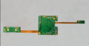
These are hybrid circuit boards that combine the features of both rigid and flexible PCBs. Rigid areas provide structural support, while flexible sections allow for dynamic movement and versatility.
This makes them invaluable in industries such as aerospace, medical devices, and consumer electronics, where design flexibility and space efficiency are paramount.
The Role of Additive Processes in PCB Fabrication
Additive processes, often referred to as 3D printing, involve building up layers of material to create a finished product, rather than subtracting material from a larger block.
In the context of PCB fabrication, these methods present several advantages over traditional subtractive techniques.
1. Design Freedom and Complexity
One of the most significant benefits of additive manufacturing is the level of design freedom it offers.
Designers are no longer constrained by the limitations of conventional PCB manufacturing.
With known designs requiring intricate shapes and layouts, additive processes allow for the creation of complex geometries and miniaturization, ultimately leading to more compact electronic devices.
This freedom encourages engineers to explore innovative configurations that optimize board functionality while reducing overall size and weight.
With rigid-flex layouts, for instance, it’s now feasible to interconnect multiple components in diverse orientations without compromising the integrity or performance of the circuit.
2. Reduced Material Waste
Traditional PCB fabrication often involves significant material waste due to terrain cutting and etching processes.
Conversely, additive methods build each component layer by layer, minimizing excess material.
This not only contributes to sustainability but also reduces costs associated with wasted materials.
Manufacturers can allocate resources more efficiently, leading to improved profit margins.
3. Microfabrication Capabilities
Additive processes excel in the field of microfabrication.
As electronics become more advanced and compact, the need for smaller, more precise components is increasingly critical.
These manufacturing methods allow for the development of fine features that are less achievable with traditional methods.
Rigid-flex PCBs can now incorporate microvias and intricate features that facilitate high-density interconnects, ultimately enhancing performance.
Instead of relying solely on bulky components, designers can integrate more complex circuits into rigid-flex structures, effectively creating a multifunctional assembly.
This is particularly beneficial in applications where space is at a premium.
4. Accelerated Prototyping
The speed and adaptability of additive processes significantly enhance the prototyping phase of PCB development.
Engineers can quickly iterate designs and fabricate prototypes in days instead of weeks, enabling faster testing and validation.
This rapid prototyping helps companies respond more effectively to market demands, giving them a competitive edge.
Additionally, the ability to easily modify designs during the prototyping stage means that issues can be addressed quickly, leading to higher overall quality in the final product.
5. Customization and Flexibility
With today’s electronic devices becoming increasingly personalized, the demand for custom PCB solutions is on the rise.
Additive manufacturing facilitates this by allowing manufacturers to easily create tailored solutions that meet specific customer requirements.
Rigid-flex designs can be customized for unique applications in a way that traditional PCB methods struggle to replicate.
This flexibility is particularly appealing in niche markets, where specialized devices may require unique functionalities that standardized PCBs cannot provide.
The Future of Rigid-Flex PCB Manufacturing
As electronic devices continue to evolve, the integration of additive processes into rigid-flex PCB fabrication will likely expand.
The potential for further innovations and enhancements in design, efficiency, and cost-effectiveness remains vast.
Companies embracing these new methodologies will be well-positioned to lead the industry forward.
Conclusion
The journey from design to reality in rigid-flex PCB fabrication is being transformed through the adoption of additive processes.
By offering unprecedented design freedom, reducing waste and costs, enhancing microfabrication capabilities, accelerating prototyping, and allowing for greater customization, these advanced manufacturing techniques are paving the way for a new era in electronics.
As technology advances, the significance of rigid-flex PCBs will only grow, making the leap to additive manufacturing not just a trend, but a necessity for companies looking to innovate and stay competitive in the ever-evolving landscape of electronics.