
Material Selection and Layer Stackup Guidelines for Rigid-Flex PCBs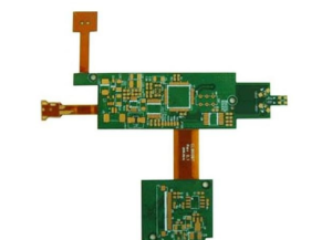
Material selection and layer stackup are critical elements in the design and manufacturing of rigid-flex PCBs (Printed Circuit Boards).
These boards combine the best characteristics of both rigid and flexible circuits, enabling versatile applications in various electronic devices, including smartphones, medical devices, and automotive systems.
Understanding the right materials and appropriate stackup can ensure functionality, durability, and manufacturability.
Understanding Rigid-Flex PCBs
Rigid-flex PCBs are hybrid circuit boards that incorporate both rigid and flexible materials, allowing for complex designs that can be folded and shaped without compromising electrical performance.
The key to creating effective rigid-flex systems lies in the optimization of material selection and carefully planned layer stackup configurations.
Material Selection: The Foundation of Quality
When it comes to material selection, there are several key factors to consider:
- Base Materials: The choice of base materials significantly affects the PCB’s performance, reliability, and fabrication process.
Common materials include FR-4, which is standard for rigid sections, and polyimide for flexible parts.
FR-4 offers excellent electrical insulation and mechanical strength, while polyimide is favored for its high-temperature resistance and flexibility. - Copper Foil: The thickness of the copper foil also plays a vital role. Thicker copper supports higher current applications, whereas thinner foils are used for miniaturization and flexible applications.
- Adhesives: Selecting the appropriate adhesive is crucial for bonding rigid and flexible layers.
Adhesives should have high thermal stability and excellent adhesion properties to ensure reliability over time. - Surface Finishes: The choice of surface finish impacts solderability and overall performance.
Immersion gold and ENIG (Electroless Nickel Immersion Gold) finishes are popular choices due to their excellent soldering characteristics and environmental resistance.
Layer Stackup Guidelines: Creating a Balanced Design
The layer stackup configuration of rigid-flex PCBs is instrumental in achieving their desired electrical and mechanical properties.
Here are some considerations to keep in mind:
1. Layer Count:
The number of layers in a rigid-flex PCB can typically vary from 2 to 12.
The design should align with the thermal and mechanical tolerances necessary for specific applications.
A higher layer count can increase complexity but allows for more versatile circuit design.
2. Alternating Rigid and Flexible Layers:
A core principle of rigid-flex design is the alternation between rigid and flexible layers.
For example, a sample stackup might consist of two rigid layers at the ends, with one or more flexible layers in between.
This arrangement maximizes flexibility while maintaining the necessary rigidity for critical components.
3. Impedance Control:
Maintaining controlled impedance is essential, especially in high-frequency applications.
The dielectric thickness and the distance between power and ground planes should be designed accordingly to prevent signal integrity issues.
4. Thermal Management:
As rigid-flex PCBs often encounter varying thermal conditions, employing thermal management techniques is vital.
A stackup design that incorporates thermal vias or materials with good thermal conductivity helps dissipate heat effectively.
Design for Manufacturability (DFM)
A crucial aspect of our discussion is the design for manufacturability.
This approach focuses on ensuring that rigid-flex PCBs are straightforward to fabricate while meeting mechanical and electrical specifications. DFM emphasizes:
- Minimizing Complexity: Simplifying the layout can reduce manufacturing costs and minimize potential errors.
- Consideration of Tolerances: Tight tolerances can lead to various challenges; proper alignment during manufacturing is critical to avoid issues in the final assembly.
- Testing and Inspection: Ensure to incorporate test points and consider future inspection requirements early in the design process.
Conclusion
Material selection and layer stackup are foundational components in the effective design of rigid-flex PCBs.
By carefully considering the materials used, shaping the stackup to fit specific application needs, and employing DFM principles, designers can create boards that not only meet functional criteria but also stand up to real-world demands. As technology continues to evolve, a clear understanding of these guidelines will become increasingly important for engineers and manufacturers alike, ensuring the success of their rigid-flex PCB designs.
The integration of innovative materials and stackup techniques will propel the development of next-generation electronics, driving efficiency and enhancing user experiences across numerous industries.